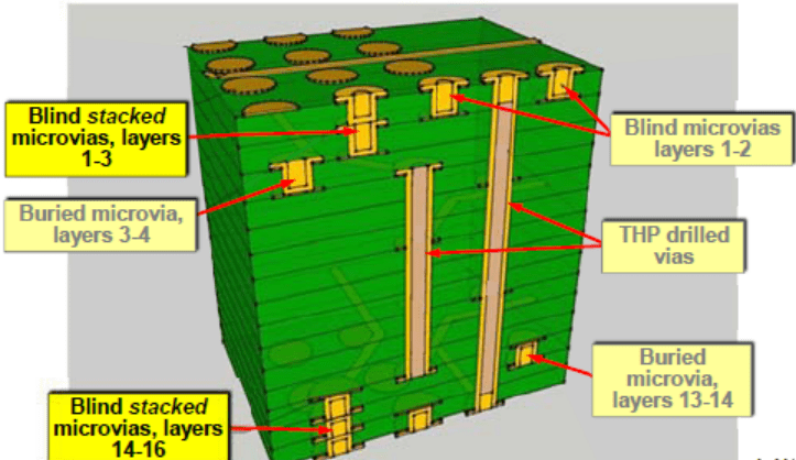
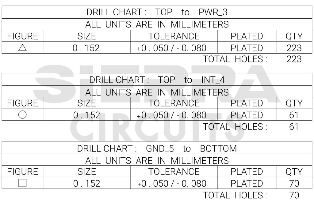
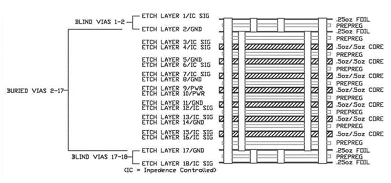
Case study: 8 and 14-layer HDI with Stacked Vias
4.5 (664) · $ 14.50 · In stock

This case study focuses on the challenges and solutions that we implemented to design complex HDI boards with stacked vias.

Multilayer PCB Stackup Planning - Engineering Technical - PCBway

What is HDI PCB?

HDI PCB Stackup - Venture Elctronics

HDI PCB Design,Manufacturing and its cost

Routing High Density Inteconnects With Reliable Microvias - 1
Case study: 8 and 14-layer HDI with Stacked Vias

Understanding Proper PCB Design (Part 2) - Circuit Cellar

Electronics, Free Full-Text
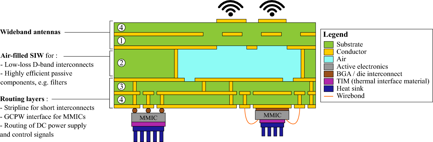
Air-filled SIW technology for mass-manufacturable and energy-efficient terahertz systems

An in-depth analysis on PCB stackup
What Is HDI PCB Design?

Ultimate HDI PCB Manufacturer in China PCBTok
Case study: 8 and 14-layer HDI with Stacked Vias
Designing HDI PCBs: The Requirements, Advantages and Complexities
Multilayer PCB Design: HDI Stackup Demystified